
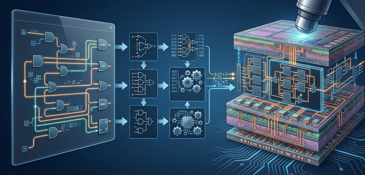
VHDL and Verilog provide a structured way to describe digital hardware, while FPGA devices turn those descriptions into configurable physical logic. The path from code to silicon passes through register transfer level design, simulation, synthesis, timing analysis, placement, routing, and device programming.
Engineers and technical managers evaluating digital design capability need to understand this complete chain. A hardware description language is not software running on a processor. Its synthesizable structures define hardware behaviour and architecture. Understanding that distinction helps organisations evaluate workforce capability, development workflows, verification requirements, and implementation quality.
For a foundational explanation of how these technologies work together, see VHDL/Verilog and FPGA devices for digital design training before evaluating implementation approaches.
How do VHDL and Verilog become physical FPGA hardware?
VHDL and Verilog become FPGA hardware through a controlled transformation from RTL descriptions to synthesised logic, followed by optimisation, placement, routing, timing verification, bitstream generation, and configuration of programmable resources inside the selected FPGA device.
The process starts with a functional requirement. An engineering team defines what the digital system must calculate, store, control, communicate, or detect. Designers then represent this behaviour using VHDL or Verilog.
The next stage is register transfer level design. RTL describes how data moves between registers and how combinational logic processes that data during clocked operation. This representation provides the bridge between the functional specification and physical implementation.
Simulation evaluates whether the RTL behaves according to its specification. A testbench supplies controlled inputs and checks resulting outputs. The design then enters synthesis, where the synthesis tool interprets synthesizable HDL structures and produces a hardware representation.
For an FPGA, that representation maps onto configurable resources. Lookup tables implement logic functions. Registers store state. Memory resources support storage requirements. Routing resources connect these elements. Dedicated clocking and input-output resources support specialised system requirements.
Implementation then determines how the resulting logic is physically arranged within the FPGA architecture. Placement assigns resources to physical locations, while routing establishes connections between them.
Timing analysis evaluates whether the implemented design meets its defined timing requirements. The resulting configuration data is then used to program the FPGA device.
This sequence makes FPGA development a transformation pipeline rather than a single coding activity.
What role does register transfer level design play between HDL and silicon?
Register transfer level design translates functional requirements into clock-driven hardware structures by defining registers, data paths, control logic, and signal relationships that synthesis tools can transform into configurable FPGA resources.
RTL sits at the centre of the digital design process. It provides enough structural detail for synthesis while remaining more abstract than a physical FPGA implementation.
A designer developing a data-processing module, for example, defines registers that capture values on clock edges. Combinational logic processes those values between clock events. Control logic determines when data is loaded, transferred, modified, or retained.
This approach creates a predictable relationship between HDL and hardware. A register described in synthesizable RTL generally corresponds to physical storage resources. Boolean expressions and conditional structures influence the logic implemented around those registers.
RTL quality therefore affects downstream implementation. Poorly structured descriptions create unnecessary resources, inefficient logic, difficult timing paths, or verification problems. Well-organised RTL supports reuse, maintainability, optimisation, and predictable synthesis.
For corporate engineering teams, this distinction is important when identifying workforce skill gaps. Knowing HDL syntax is not equivalent to understanding RTL architecture. Effective capability includes the ability to translate specifications into synchronous hardware structures and assess the implementation consequences.
How does synthesis translate VHDL and Verilog into FPGA resources?
Synthesis analyses synthesizable VHDL or Verilog, interprets its hardware intent, optimises the logic, and generates an implementation-oriented representation using resources such as lookup tables, registers, memory blocks, and other FPGA-specific structures.
Synthesis is the stage where HDL descriptions become an explicit hardware architecture for implementation.
The synthesis engine analyses constructs such as conditional statements, arithmetic operations, state machines, registers, multiplexers, and Boolean expressions. It then determines suitable FPGA resources for implementing those structures.
Consider a simple conditional expression. Depending on its structure and the target architecture, synthesis can implement the resulting logic through lookup tables or combinations of dedicated resources. A clocked process describing stored state results in register-based hardware.
Synthesis also performs optimisation. Redundant logic can be removed. Equivalent expressions can be simplified. Constant values can be propagated. Logic can be reorganised to improve resource usage or performance.
The synthesis report therefore provides useful engineering information. Teams can examine resource utilisation and identify whether the resulting architecture aligns with project expectations.
This is an important evaluation point when comparing learning approaches. Training that focuses exclusively on HDL syntax does not address the relationship between code and synthesised hardware. Practical development requires engineers to interpret synthesis results and adjust RTL accordingly.
Why do lookup tables matter when mapping RTL to FPGA architecture?
Lookup tables provide configurable logic resources inside many FPGA architectures, allowing synthesised Boolean functions and related logic structures to be implemented efficiently while influencing resource utilisation, routing requirements, and overall design performance.
Lookup tables are fundamental building blocks in many FPGA architectures. Instead of constructing every Boolean function from fixed physical gates, the FPGA configures memory-like logic resources to represent required functions.
When synthesis identifies a logic function, the implementation process determines how that function fits into available lookup-table resources. Larger or more complex functions can require multiple resources and additional routing.
This creates an important relationship between RTL structure and physical architecture. Two descriptions that produce identical functional outputs can generate different implementation characteristics.
Resource utilisation therefore becomes a practical design consideration. Engineers examine synthesis and implementation reports to determine how much of the available architecture is consumed.
In large corporate projects, this information affects scalability. A design that uses a substantial proportion of available resources has less capacity for future features. Resource-efficient RTL provides greater architectural flexibility.
How should testbenches be evaluated before synthesis?
Testbenches should verify functional behaviour against defined requirements before implementation, using controlled stimulus, expected results, assertions, boundary conditions, and repeatable scenarios that expose logic errors before hardware deployment.
A testbench provides a controlled environment for exercising an RTL design without requiring physical hardware for every validation cycle.
Effective testbench development begins with requirements. Engineers identify expected inputs, outputs, operating conditions, exceptional cases, and timing relationships. Test scenarios then represent those requirements in a repeatable form.
Simulation results can reveal incorrect state transitions, unexpected outputs, missing conditions, arithmetic errors, and interface problems. Waveform analysis helps engineers trace how signals change over time.
A testbench also supports regression testing. When a design changes, previously validated scenarios can be executed again to detect unintended effects.
For organisations, verification capability has direct implications for development efficiency. Errors detected during simulation are generally easier to isolate than faults discovered after physical implementation. A structured verification process therefore forms an important part of workforce capability assessment.
How do timing constraints affect the transition from RTL to a working FPGA?
Timing constraints define the performance requirements that implementation must satisfy, including clock relationships and input-output timing, enabling tools to analyse whether data reaches its required destinations within the available timing budget.
Functional correctness does not guarantee timing correctness. A design can produce the expected logical result while failing to operate reliably at its required clock frequency.
Timing constraints communicate system requirements to FPGA development tools. Clock definitions establish the expected operating periods. Input and output constraints describe relationships with external interfaces. Additional constraints define relationships between clock domains and other timing conditions.
After synthesis and implementation, timing analysis evaluates paths through the design. Setup and hold requirements determine whether data arrives within acceptable windows around clock events.
A failed timing result requires engineering investigation. Designers can restructure RTL, reduce logic depth, modify pipeline stages, adjust clocking architecture, or reconsider resource usage.
Timing therefore becomes an evaluation criterion when organisations assess digital design capability. Professionals need to understand not only how to write HDL but also how implementation results affect system performance.
What does Xilinx Vivado add to the FPGA development workflow?
Xilinx Vivado integrates design entry, simulation, synthesis, implementation, constraint management, timing analysis, and programming activities into a development environment that connects HDL descriptions with implementation results for supported FPGA devices.
Xilinx Vivado provides a practical environment for managing multiple stages of FPGA development. Rather than treating HDL, synthesis, constraints, and implementation as separate activities, engineers work through a connected toolchain.
A typical workflow begins with project configuration and RTL source files. Designers then run simulation, review functional behaviour, execute synthesis, inspect resource utilisation, apply timing constraints, and proceed to implementation.
Implementation generates reports covering resource usage, placement, routing, and timing. These reports create feedback for further design refinement.
This workflow also helps organisations standardise engineering practices. Teams can establish common project structures, constraint management procedures, verification practices, reporting conventions, and design review checkpoints.
For HR and L&D teams, tool-specific capability is therefore best evaluated alongside underlying engineering knowledge. A professional who understands Vivado menus without understanding RTL, synthesis, timing, and FPGA architecture has limited ability to diagnose implementation problems.
Which FPGA learning approach builds capability from HDL to implementation?
An effective learning approach connects HDL syntax with RTL architecture, simulation, synthesis, FPGA resources, timing constraints, implementation reports, and debugging so participants understand the complete engineering chain rather than isolated development activities.
Learning methods differ in how closely they reproduce the actual development lifecycle.
A theory-led approach can establish important concepts such as digital logic, synchronous design, HDL syntax, and FPGA architecture. It provides the conceptual foundation required for technical communication.
A tool-led approach focuses on development environments and practical workflows. Participants gain familiarity with project creation, simulation, synthesis, constraints, and implementation.
A project-based approach connects these elements through a complete design problem. Participants begin with a specification, create RTL, build a testbench, simulate behaviour, synthesise the design, analyse resource usage, apply timing constraints, implement the design, and investigate results.
For professional development, the third approach creates stronger alignment with workplace workflows because it exposes the dependencies between each stage.
The appropriate learning structure depends on the workforce gap. New entrants require stronger foundational concepts. Experienced engineers often require optimisation, verification, timing, or architecture-focused development. Technical managers need enough system understanding to evaluate project dependencies and delivery risks.
How should organisations evaluate FPGA training effectiveness?
Organisations should evaluate FPGA training through technical capability, implementation quality, verification performance, resource utilisation, timing results, development workflow consistency, and the ability to transfer learned methods into real engineering projects.
Training effectiveness should extend beyond attendance or completion rates.
Technical assessments can measure whether participants create synthesizable RTL, construct effective testbenches, interpret synthesis reports, apply timing constraints, and diagnose implementation problems.
Project-based assessment provides another useful measurement. Participants can complete a defined FPGA design task and demonstrate the complete workflow from specification to implementation.
Organisations can also monitor engineering indicators after training. These include verification cycle efficiency, recurring design errors, timing-closure performance, resource utilisation, documentation quality, and adherence to development standards.
ROI assessment should connect learning outcomes with business requirements. If an engineering team needs stronger FPGA verification capability, the relevant measurement focuses on verification quality and defect detection rather than general course completion.
This approach gives HR teams and technical managers a clearer basis for evaluating professional development investment.
When is structured professional training appropriate for VHDL, Verilog and FPGA development?
Structured professional training is appropriate when organisations need consistent capability across HDL development, RTL architecture, verification, synthesis, timing, FPGA implementation, and engineering workflow management rather than isolated knowledge of programming syntax.
Corporate training becomes relevant when workforce capability must support defined engineering outcomes.
A team moving from software-oriented development into programmable hardware needs foundational digital design knowledge. An existing FPGA team facing recurring timing failures needs stronger timing analysis and RTL optimisation capability. A growing engineering department needs common development standards and repeatable workflows.
The delivery model should reflect these requirements. Instructor-led sessions support guided technical explanation and discussion. Practical labs connect concepts with tools. Project work demonstrates application. Assessments identify remaining skill gaps.
For organisations requiring a broader technical development pathway, Information Technology and Programming Courses provide a wider professional training context in which specialised digital design capability can sit.
The key evaluation principle is alignment. Training content, delivery method, assessment criteria, and business objectives need to address the same workforce requirement.
How should organisations decide between HDL knowledge and complete FPGA capability?
Organisations should distinguish basic HDL knowledge from complete FPGA capability by assessing whether professionals can move independently from functional requirements through RTL design, verification, synthesis, timing analysis, implementation, debugging, and documented engineering delivery.
This distinction prevents training decisions from focusing too narrowly on language syntax.
A professional who understands VHDL or Verilog constructs can produce code. A capable FPGA designer understands what that code represents as hardware, how synthesis interprets it, how resources are consumed, how timing behaves, and how implementation results influence subsequent design decisions.
The evaluation should therefore follow the complete workflow.
First, assess digital design fundamentals. Next, evaluate RTL architecture. Then assess simulation and testbench development. Follow this with synthesis interpretation, resource analysis, timing constraints, implementation, and debugging.
The final measure is transfer to workplace projects. Professionals need to apply the same reasoning to actual technical requirements, development standards, review processes, and delivery constraints.
When the evaluation shifts from knowledge acquisition to implementation readiness, a structured programme such as Turn VHDL/Verilog and FPGA Devices Theory Into Working Silicon with The British Academy for Training and Development becomes the relevant decision-stage resource.
How does the complete HDL-to-silicon workflow support business objectives?
The complete HDL-to-silicon workflow supports business objectives by creating a repeatable path from technical requirements to verified programmable hardware, improving development control, resource visibility, timing assurance, engineering consistency, and workforce capability.
FPGA development combines software-like design flexibility with hardware implementation requirements. Organisations therefore need professionals who understand both abstraction and physical consequences.
A disciplined workflow reduces disconnected decision-making. Requirements guide RTL architecture. RTL drives synthesis. Synthesis reveals resource usage. Constraints define timing requirements. Implementation exposes physical results. Verification and debugging feed improvements back into the design.
This creates a continuous engineering loop.
For HR teams, the implication is that digital hardware training should be mapped to specific competency requirements. For engineering managers, it means training outcomes should correspond to measurable technical tasks. For organisations, it means learning investment can be assessed against project capability rather than attendance alone.
Explore More Expert Insights:
Radio Jamming Techniques Explained: Barrage, Spot and Sweep Signatures
Software Defined Radio Platforms Compared: RTL-SDR, HackRF and USRP for Practical Applications
The relationship between VHDL, Verilog, FPGA devices, RTL, synthesis, testbench development, timing constraints, lookup tables, and implementation is therefore the central consideration. Understanding that relationship enables more precise decisions about workforce development and digital hardware engineering capability.