
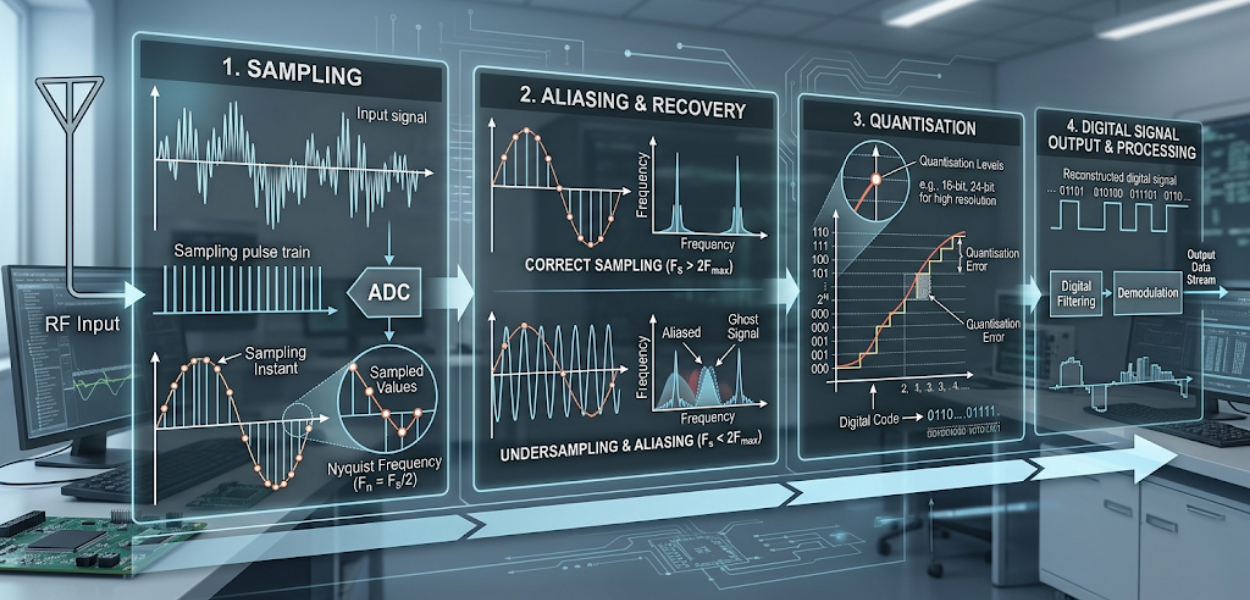
Digital signal processing in communication receivers depends on converting continuous analogue signals into digital representations without losing information that the receiver needs for detection, demodulation, filtering and analysis. Sampling, aliasing and quantisation form the core of this conversion chain because each stage directly affects signal fidelity and receiver performance.
For organisations developing technical capability, understanding Digital Signal Processing for Communication Systems Training Courses provides the broader foundation for evaluating how DSP concepts translate into practical communication-system workflows. Within that foundation, sampling rate, anti-aliasing design and quantisation resolution require particular attention because errors introduced at the receiver input propagate through later processing stages.
Why does sampling determine the quality of digital communication receiver processing?
Sampling determines how accurately a receiver represents an analogue waveform in digital form, with the sampling rate defining the highest recoverable frequency and influencing subsequent filtering, demodulation, storage and computational requirements.
A communication receiver receives signals as continuous-time waveforms. An analogue-to-digital converter then takes measurements at discrete time intervals. The number of measurements taken per second is the sampling rate, expressed in samples per second or hertz.
The sampling theorem states that a band-limited signal requires a sampling frequency greater than twice its highest frequency component for ideal reconstruction. This minimum is called the Nyquist rate.
For example, a receiver processing a signal with frequency content extending to 5 MHz requires a sampling frequency above 10 MHz under the ideal conditions described by the theorem. Practical receiver designs use additional margin because real filters do not provide an infinitely sharp frequency boundary.
Sampling decisions also affect system resources. Increasing the sampling frequency generates more digital samples. More samples increase processor workload, memory requirements, data-transfer rates and storage requirements.
For corporate engineering teams, the decision therefore extends beyond signal theory. Training managers evaluating DSP capability need to consider whether engineers understand the relationship between signal bandwidth, ADC configuration, processor capacity and receiver performance.
A technically correct sampling strategy starts with identifying the information-bearing bandwidth rather than selecting a sampling rate independently of the receiver architecture.
How does oversampling affect receiver design?
Oversampling uses a sampling frequency substantially higher than the minimum required by the signal bandwidth. It creates additional frequency separation between the desired signal and unwanted spectral components.
This separation makes analogue anti-aliasing filters easier to implement because the transition band becomes wider. Oversampling also supports later digital filtering and rate conversion.
The trade-off is computational and data-rate overhead. A receiver processing millions of additional samples per second requires corresponding processing capacity. The appropriate rate therefore depends on bandwidth, converter capability, digital architecture and downstream algorithms.
What causes aliasing in a communication receiver?
Aliasing occurs when frequency components above half the sampling frequency are represented as lower-frequency components after sampling, creating irreversible spectral distortion that digital processing cannot remove once the samples have been captured.
Aliasing happens when the sampling frequency is insufficient for the signal spectrum reaching the ADC. Frequency components outside the permissible range fold into the digital baseband.
Suppose a receiver samples at 20 MHz. Its Nyquist frequency is 10 MHz. A 13 MHz component entering the converter does not remain represented at 13 MHz because that frequency lies above the Nyquist limit. Its sampled representation appears at 7 MHz.
This phenomenon is particularly important in communication receivers because interference, adjacent-channel energy and unwanted harmonics can enter the ADC alongside the desired signal.
Once aliasing occurs, the receiver cannot distinguish the aliased component from a legitimate lower-frequency signal using ordinary digital processing. The problem therefore has to be addressed before conversion.
Why are anti-aliasing filters necessary?
An anti-aliasing filter is an analogue low-pass or band-limiting filter positioned before the ADC. Its purpose is to attenuate frequency components that would otherwise fold into the usable digital spectrum.
The filter design depends on:
A higher sampling frequency provides greater separation between the desired spectrum and the Nyquist boundary. This reduces the filtering demands placed on the analogue stage.
Receiver engineers therefore evaluate sampling and filtering together rather than treating them as separate design decisions.
How does quantisation affect digital receiver accuracy?
Quantisation converts each sampled amplitude into one of a finite number of digital levels, introducing quantisation error that influences signal-to-noise performance, dynamic range, weak-signal detection and the accuracy of later digital processing.
Sampling discretises time, while quantisation discretises amplitude. An ADC with a finite number of bits cannot represent every possible analogue amplitude exactly.
For an ideal N-bit converter, the number of quantisation levels is:
2ᴺ
An 8-bit ADC provides 256 levels. A 12-bit ADC provides 4,096 levels. A 16-bit ADC provides 65,536 levels.
Increasing resolution reduces the spacing between adjacent quantisation levels. Under ideal assumptions, each additional ADC bit increases theoretical signal-to-quantisation-noise performance by approximately 6.02 dB.
Quantisation becomes particularly important when receivers process weak signals alongside strong interference. Limited resolution can reduce the ability to distinguish small signal variations from quantisation effects.
The effective performance of a real ADC also depends on factors beyond nominal bit depth. Noise, non-linearity, clock jitter and analogue front-end limitations influence the actual result.
What is quantisation noise?
Quantisation noise represents the difference between the original sampled amplitude and the quantised value. For an ideal uniform quantiser, this error is commonly modelled as noise when the signal exercises enough quantisation levels.
This model supports practical analysis of signal-to-quantisation-noise ratio. It becomes less representative when signals are extremely weak, highly structured or poorly distributed across the converter range.
Receiver engineers therefore need to evaluate quantisation relative to the actual signal environment rather than interpreting ADC resolution as an isolated specification.
How should sampling and quantisation be evaluated together?
Sampling determines when signal information is captured, while quantisation determines how precisely each captured amplitude is represented; receiver performance depends on selecting both parameters according to bandwidth, dynamic range and processing requirements.
A receiver with a high sampling rate but inadequate amplitude resolution still produces inaccurate digital data. A high-resolution ADC operating at an inappropriate sampling rate still produces aliased information.
The two parameters address different dimensions of conversion:
This relationship is important when organisations assess technical skill gaps. Engineers working with communication receivers need to understand the complete conversion chain instead of memorising isolated DSP definitions.
How do FIR filters support receiver processing after sampling?
Finite impulse response filters process sampled signals using a finite sequence of coefficients, providing controlled frequency responses and predictable behaviour for channel selection, anti-aliasing stages in digital domains and signal conditioning.
An FIR filter applies weighted combinations of current and previous input samples. Its coefficients determine the filter's frequency response.
FIR filters are widely used because they can provide linear-phase characteristics and stable finite-duration responses. These properties are valuable when preserving waveform relationships is important.
In a receiver, an FIR filter can isolate a required channel, suppress unwanted frequency components or prepare a signal for sample-rate conversion.
The computational cost depends on filter length and sampling frequency. A longer filter generally provides greater control over the transition band but requires more multiplication and accumulation operations.
This creates an engineering trade-off between filtering precision and computational efficiency.
When are FIR filters useful before decimation?
Decimation reduces the sampling rate after digital processing. Before reducing the rate, unwanted frequency components must be removed to prevent aliasing during the new sampling process.
A digital low-pass FIR filter therefore commonly precedes a decimation stage. The filter restricts the spectrum to the range that the lower sampling rate can represent safely.
For example, reducing a sample rate by a factor of four requires the digital signal to be appropriately band-limited before the reduction. Otherwise, spectral components that were acceptable at the original rate can fold into the new digital spectrum.
What role does the fast Fourier transform play in receiver analysis?
The fast Fourier transform converts sampled time-domain data into a frequency-domain representation efficiently, allowing engineers to examine spectral occupancy, interference, harmonics, filter behaviour and signal components within communication receivers.
The discrete Fourier transform provides frequency-domain information from sampled data. The fast Fourier transform is an efficient algorithm for calculating that transform.
FFT analysis helps receiver engineers identify:
The FFT does not replace correct sampling. If the original data contains aliasing, the frequency-domain display represents the aliased signal rather than reconstructing the missing information.
This distinction matters in troubleshooting. A spectral peak appearing at an unexpected frequency can originate from genuine interference, sampling-related aliasing, oscillator behaviour or another stage of the signal chain.
FFT interpretation therefore requires knowledge of the receiver's sampling architecture.
How does the z-transform support digital receiver filter analysis?
The z-transform represents discrete-time signals and systems mathematically, allowing engineers to analyse digital filters, poles, zeros, stability and frequency response within the sampled signal-processing environment.
The z-transform provides a framework for describing discrete-time systems using complex-variable representations.
For digital filters, it helps engineers examine transfer functions and understand how coefficients influence system behaviour. It also supports the analysis of infinite impulse response filters and other discrete-time systems.
Although FIR filters do not require feedback to operate, z-domain analysis remains useful for understanding digital filtering concepts and frequency response.
For professional teams, this mathematical foundation connects implementation with system behaviour. Engineers can move from an observed frequency response to the underlying filter structure and then assess whether the design meets receiver requirements.
How should organisations evaluate DSP learning approaches for receiver teams?
Effective DSP learning for receiver teams combines mathematical foundations with practical signal-processing tasks, enabling engineers to connect sampling theory, aliasing, quantisation, filtering and spectral analysis with measurable receiver performance.
A purely theoretical learning approach develops terminology and mathematical understanding. A practical approach adds implementation and troubleshooting experience.
For organisations, the choice depends on the workforce's existing capability and job requirements.
Engineers working directly with receiver algorithms require deeper technical practice. Technical managers need enough DSP knowledge to interpret engineering decisions and performance measurements. HR and L&D teams need a clear connection between training outcomes and workplace responsibilities.
Useful learning outcomes include the ability to:
Performance measurement should focus on demonstrable technical outcomes rather than course completion alone.
For example, an organisation can assess whether participants correctly diagnose aliasing in a simulated receiver, select appropriate filtering parameters and explain how ADC resolution affects the signal chain.
How can DSP capability be measured after technical training?
DSP capability is best measured through applied engineering tasks that test signal analysis, parameter selection, troubleshooting and interpretation rather than relying only on attendance, assessment scores or completion certificates.
A workforce assessment can begin with a baseline test covering sampling, quantisation and frequency-domain concepts. A post-training assessment can then use equivalent technical scenarios.
Relevant performance indicators include:
The measurement period should reflect the complexity of the role. Immediate testing measures knowledge acquisition. Later workplace assessments measure whether engineers apply that knowledge to receiver development and troubleshooting.
This approach gives HR and L&D teams a clearer connection between technical learning and operational performance.
How should teams select a practical DSP solution for receiver problems?
Teams should select a DSP learning or implementation approach according to receiver architecture, signal bandwidth, existing engineering capability, computational constraints and measurable performance requirements rather than selecting techniques independently.
The decision begins with the receiver's signal path.
Engineers identify the analogue bandwidth, expected interference, ADC characteristics and required digital output. They then determine the appropriate sampling strategy and filtering requirements.
After conversion, digital processing requirements determine whether FIR filtering, FFT analysis, decimation or additional mathematical methods are necessary.
For teams moving from theory into applied receiver work, a practical programme focused on real signal-processing scenarios provides a direct way to connect these concepts with implementation tasks. Apply Digital Signal Processing to Real Receiver Problems at The British Academy for Training and Development fits at this point because the reader has already moved from understanding DSP principles toward evaluating their application to receiver problems.
The wider technical learning pathway can also sit within Information Technology and Programming Courses, particularly where DSP capability forms part of broader digital engineering and programming responsibilities.
Explore More Expert Insights:
Antenna Design and Measurement: Gain, Directivity and Radiation Pattern Fundamentals
IP Protocols and Technologies: Encapsulation, MTU and Path Discovery Explained
The selection process should then consider whether the learning environment provides relevant simulations, signal-analysis exercises, receiver scenarios and measurable technical outcomes.
A useful evaluation sequence is straightforward:
This approach keeps DSP development connected to actual engineering responsibilities.